+91 90324 21995 [email protected] Tirupati, Andhra Pradesh
+91 90324 21995

RTL Design Course

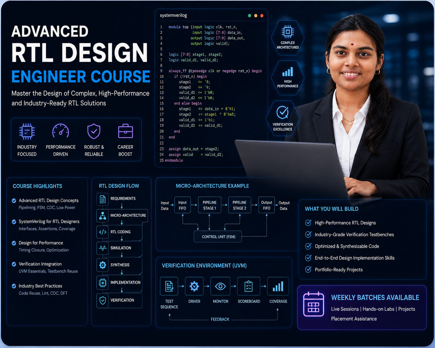
Master Digital Design, Verilog HDL, RTL Design, FSMs, Memory Design, and FPGA Implementation to build industry-ready VLSI design skills through hands-on projects, expert mentorship, and real-world applications. Gain practical experience with industry-standard design methodologies and accelerate your
4.8/5 Student Rating
5,000+ Students Trained
200+ Hiring Partners
Weekly Batches Available

ADVANCED RTL DESIGN ENGINEER

Duration: 6 Months
Mode: Online / Offline
Language: English, Telugu, Tamil, Hindi
Industry-Recognized Certification from Takeoff Training Institute
Python for Data Science
Machine Learning
Deep Learning
Data Visualization
AI & Neural Networks
Model Deployment
Real Industry Projects
Placement Support
Pandas & NumPy
Statistics & Probability
Python for Data Science
Machine Learning
Deep Learning
Data Visualization
AI & Neural Networks
Model Deployment
Real Industry Projects
Placement Support
Pandas & NumPy
Statistics & Probability
Course Curriculum

Comprehensive ADVANCED RTL DESIGN ENGINEER Curriculum

The RTL Design Using Digital Electronics and Verilog HDL program is designed to provide strong fundamentals and practical skills required for VLSI Front-End Design, FPGA Design, and RTL Engineering roles. The curriculum covers Digital Electronics, Boolean Algebra, Logic Minimization, Combinational and Sequential Circuits, FSM, Memory Design, FIFO, and FPGA fundamentals. Learners gain hands-on experience in designing Adders, Multipliers, MUX, Registers, Counters, ALU, and Control Logic circuits. The Verilog HDL module focuses on RTL coding, modeling techniques, testbench development, simulation, debugging, and synthesis-aware design practices. Through practical labs and industry-oriented projects, learners develop skills in creating reusable, scalable, and synthesizable hardware designs. The program also includes FPGA implementation, mini projects, interview preparation, and placement support for careers in the semiconductor industry.

Detailed Syllabus

Digital Electronics Fundamentals

Types of Number Systems and Representation
Binary Number System
Octal and Hexadecimal Number Systems
Base Conversions
Decimal to Binary
Octal
Hexadecimal
Binary to Octal and Hexadecimal
Number System Arithmetic
Addition
Subtraction
Multiplication
Division
Negative Number Representation
Sign Magnitude Representation
Complement Systems
1’s Complement
2’s Complement
9’s Complement
10’s Complement
Complement Arithmetic
Addition and Subtraction
Overflow Detection
BCD Complement Arithmetic

Digital Codes

Types of Binary Codes
Weighted Codes
BCD Code
2421 Code
5211 Code
Non-Weighted Codes
Alphanumeric Codes
Sequential Codes
Self-Complementing Codes
Cyclic Codes
Excess-3 Code (XS-3)
Gray Code
Error Detecting Codes
Error Correcting Codes
Hamming Code
Parity Bit Generator and Checker
ASCII Code
EBCDIC Code
Code Conversion Techniques

Logic Gates and Boolean Algebra

Basic Logic Gates
AND Gate
OR Gate
NOT Gate
Universal Gates
NAND Gate
NOR Gate
Logic Function Realization using Universal Gates
Complex Gates
Alternate Logic Gates
Two-Level Logic Realization
Tri-State Logic Gates
Logic Diagram Analysis
AND/OR/INV Conversion to NAND/NOR Logic
Pulsed Operation of Logic Gates

Boolean Algebra

Laws of Boolean Algebra
Principle of Duality
De Morgan’s Theorems
Boolean Expression Simplification

Logic Minimization Techniques

Minterms and Maxterms
SOP and POS Forms
Standard SOP and POS Conversion
Karnaugh Map (K-Map)
Two Variable K-Map
Three Variable K-Map
Four Variable K-Map
Five Variable K-Map
Six Variable K-Map
Don't Care Conditions
Hybrid Logic Optimization
SOP Minimization
POS Minimization
Multiple Output Circuit Minimization
Variable Mapping
Quine-McCluskey Method

Combinational Circuit Design

Introduction to Combinational Circuits
Difference Between Combinational and Sequential Circuits
Transmission Circuits

Arithmetic Circuits

Half Adder
Full Adder
Half Subtractor
Full Subtractor
Ripple Carry Adder (RCA)
Carry Look-Ahead Adder (CLA)
Carry Select Adder (CSLA)
Carry Skip Adder (CSKA)

Multiplier Architectures

Binary Multiplier
Booth Multiplier
Wallace Tree Multiplier
Dadda Multiplier
Signed Multiplier

Data Processing Circuits

Multiplexer (MUX)
Demultiplexer (DEMUX)
Encoder
Decoder
Comparator

Sequential Circuit Design

Types of Sequential Circuits
Clock Signals
Triggering Techniques
SR Latch
JK Latch
D Latch
T Latch
Gated Latches
SR Flip-Flop
JK Flip-Flop
D Flip-Flop
T Flip-Flop
Master-Slave JK Flip-Flop
Race Around Condition
Flip-Flop Conversion Techniques

Registers, Counters, FSM & Memory Design

Shift Registers
Bidirectional Shift Registers
Universal Shift Registers
Binary Counter
Asynchronous Counter
Synchronous Counter
Up Counter
Down Counter
Up/Down Counter
Non-Binary Counters
Ternary Counter
Quaternary Counter
Gray Code Counter
Decimal Counter
FSM Fundamentals
Mealy FSM
Moore FSM
Sequence Detector Design
Memory Classification
Memory Characteristics
RAM Architecture
ROM Architecture
Synchronous FIFO
Asynchronous FIFO
PLD
PAL
PLA
FPGA Architecture Basics

Verilog HDL Programming

Introduction to Verilog HDL
Lexical Conventions
Data Types
Modules and Ports
Writing Verilog Testbench
Gate Level Modeling
Data Flow Modeling
Behavioral Modeling
Switch Level Modeling
Verilog Operators
Blocking Assignment
Non-Blocking Assignment
Sequential Logic Implementation
Procedural Timing Control
if Statement
case Statement
Loops
Verilog Blocks
Tasks and Functions
Scheduling Semantics
System Tasks
Compiler Directives
Parameters
Procedural Continuous Assignment
Signal Strength
Generate Blocks
User Defined Primitives (UDP)

Verilog RTL Design Implementation

Half Adder
Full Adder
Half Subtractor
Full Subtractor
4-bit Ripple Carry Adder
Carry Look-Ahead Adder
Carry Select Adder
Carry Skip Adder
Binary Multiplier
Booth Multiplier
Wallace Tree Multiplier
4:1 Multiplexer
1:4 Demultiplexer
Priority Encoder
Decoder
Comparator
SR Flip-Flop
D Flip-Flop
JK Flip-Flop
T Flip-Flop
Master-Slave JK Flip-Flop
SISO Register
SIPO Register
PISO Register
PIPO Register
Universal Shift Register
Asynchronous Counter
Synchronous Counter
MOD-10 Counter
Up/Down Counter
Gray Code Counter

FSM, Memory & System-Level RTL Design

Mealy Sequence Detector
Moore Sequence Detector
Overlapping Sequence Detector
Non-Overlapping Sequence Detector
Traffic Light Controller
Synchronous FIFO Design
Asynchronous FIFO Design
Single Port RAM
ROM Design
4-bit ALU Design

RTL Verification & Advanced Coding Practices

Self-Checking Testbench Development
Adder Verification
Counter Verification
FSM Verification
FIFO Verification
Multiplier Verification
Parameterized MUX and Decoder
Parameterized FIFO Design
Parameterized Counter Design
Generate Block-Based Adder
Generate Block-Based Comparator
UDP-Based Logic Design
CMOS Switch-Level Modeling
Multi-Module ALU Verification
Multi-Module FIFO Verification
Waveform Analysis and Debugging
RTL Debugging Techniques
RTL Coding from Specifications
Combinational RTL
Sequential RTL
Synthesis-Aware Coding Practices
Technologies

Key Tools You'll Master

Master industry-leading RTL design tools including Xilinx Vivado, ModelSim, and QuestaSim through hands-on Verilog HDL projects, FPGA implementation, RTL simulation, synthesis, timing analysis, and real-world ASIC/FPGA design applications.


QuestaSim
ModelSim
Xilinx Vivado

Course Schedule

India Standard Time (IST)

Duration
6 Months
Total Hours
150+ Hours
Weekly Hours
12h per week
Classes per Week
6 sessions
Course Features

What's Included

Everything you need to succeed - from day one to your first job offer.

Industry-Oriented Curriculum

Learn SPICE simulation concepts through an industry-focused curriculum covering circuit analysis, simulation techniques, and debugging methodologies.

Hands-on Schematic Design

Gain practical experience in creating circuit schematics and understanding design flow using professional EDA environments.

Circuit Simulation Practice

Perform practical circuit simulations to verify functionality, analyze performance, and understand circuit behavior.

LTspice Training

Learn LTspice simulation techniques including circuit setup, analysis methods, parameter evaluation, and result interpretation.

Tanner EDA Training

Get hands-on exposure to Tanner EDA tools for schematic capture, simulation, and analysis of electronic circuits.

Cadence Virtuoso Training

Understand Cadence Virtuoso simulation workflows and gain practical knowledge of industry-standard analog design environments.

Waveform Analysis

Analyze simulation waveforms to evaluate circuit performance, identify issues, and validate design functionality.

Simulation Debugging Techniques

Develop skills to identify simulation errors, troubleshoot circuit issues, and improve design accuracy.

Mini Projects

Work on simulation-based mini projects to apply concepts and build confidence in circuit analysis and verification.

Interview Preparation

Prepare for VLSI and electronics industry interviews with technical discussions, simulation-based questions, and mock interview guidance.

Course Completion Certificate

Receive a course completion certificate validating your SPICE simulation and debugging skills for professional growth.

Certification

Course Completion Certificate

Earn an industry-recognized certificate upon successfully completing the program.

Course Completion Certificate
Recognized Professional Certificate
Start Your Career

Ready to Launch Your Career?

Talk to our training advisors and get a personalized learning roadmap, course fee details, batch schedule, and career guidance - all for free.

Free 1-on-1 Career Consultation
Personalized Learning Roadmap
Course Fee & EMI Details
Upcoming Batch Schedule
Free Demo Class Booking

Talk to a Career Expert

Fill in your details - our advisor will contact you within 24 hours.